When you train a defect classification model on a dataset built primarily from 300mm logic and memory fabs, you get a model that's very good at logic and memory defects. Bring that model to a 200mm BCD power fab, or a MEMS sensor foundry, or an RF BiCMOS fab running at 180nm, and you'll find that it classifies most patterns correctly most of the time — but misclassifies exactly the patterns that matter most for yield in those nodes.
This isn't a model quality problem. It's a training distribution problem. Analog and power-device fabs have genuinely different dominant defect mechanisms. Understanding what those mechanisms are, and how they appear in wafer map data, is the starting point for building a classifier that works in these environments.
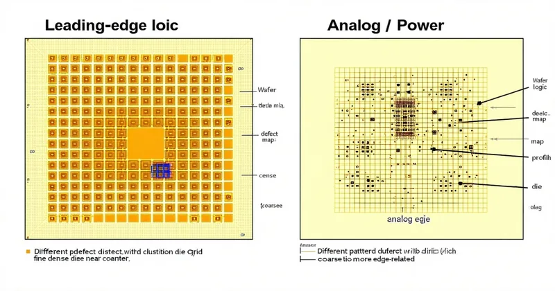
Why Analog and Power Nodes Are Structurally Different
Leading-edge logic fabs are defined by litho complexity: EUV exposure, multi-patterning, extremely tight overlay budgets. The dominant defect failure modes are litho-related — exposure dose variation, alignment shifts, mask defect replication. Wafer map patterns in logic are heavily weighted toward periodic (reticle-step) structures and spatial patterns that track photolithography field boundaries.
Analog and power nodes run on different physics. A 200mm BCD process — used for power management ICs, motor drivers, and automotive-grade linear regulators — combines bipolar, CMOS, and DMOS devices in the same substrate. The process steps that cause yield loss here are different:
- Deep N-well and P-well implants at high dose create stress fields that promote slip line defects during high-temperature drive-in. Slip lines appear as linear patterns of crystallographic origin, not lithography-induced — they follow <110> and <100> crystal directions and have a characteristic diagonal-or-axial orientation on the wafer map.
- Thick field oxide (LOCOS or STI in older BCD) causes significant topography. CMP planarization over this topography generates edge-of-field polish non-uniformity, producing a
CMP_FIELD_EDGEpattern that is distinct from theRING_EDGE_EXCLpattern seen in logic — it's field-edge-relative, not wafer-edge-relative. - High-voltage gate oxide growth (typically 50–150 Å thicker than standard CMOS gate oxide) is sensitive to furnace tube contamination. A single contamination event in the HV gate oxide furnace can produce a
FURNACE_CLUSTERpattern that correlates with wafer position within the boat, creating a non-random cluster signature that a generic model may misidentify as random particulate.
LDMOS devices — the building block of high-side power switches and RF power amplifiers — add another failure mode: body diode punch-through at high forward bias, which shows up in wafer sort as localized bin-2 fails in a spatial pattern tied to the source/drain implant gradient. These are LDMOS_BODY_RING patterns in our taxonomy — concentric ring structures that look similar to RING_EDGE_EXCL but are centered on reticle fields, not the wafer edge.
A Concrete Scenario: BCD Process, 200mm, Power Management IC
Consider a hypothetical 200mm BCD fab — the kind of facility running 250nm design rules for automotive power ICs, AEC-Q100 Grade 0 qualified. In our internal validation work modeling this node family's defect distributions, the top-5 yield-impacting pattern classes by frequency were:
| Pattern class | Spatial type | Typical process origin | Generic model accuracy |
|---|---|---|---|
RING_EDGE_EXCL | Ring / edge | CMP edge loading, bevel etch | High (well-covered by generic training data) |
SLIP_LINE_THERMAL | Linear / diagonal | High-temp anneal, crystal slip | Low (rarely seen in logic training data) |
FURNACE_CLUSTER_HV | Clustered / field-relative | HV gate oxide furnace contamination | Low (misclassified as random) |
CMP_FIELD_EDGE | Periodic / field-relative | CMP topography at field boundaries | Medium (partial overlap with LITHO_REPEAT) |
LDMOS_BODY_RING | Ring / field-relative | LDMOS body implant gradient | Low (confused with RING_EDGE_EXCL) |
The pattern here is not subtle: three of the five highest-impact classes have low accuracy on a generic model. This isn't because the patterns are visually ambiguous — a trained yield engineer recognizes SLIP_LINE_THERMAL immediately from its orientation and consistent width. The model misses it because it was never trained on enough examples of this pattern type to learn the distinguishing features.
MEMS and RF Nodes: Even Further from the Training Distribution
MEMS fabs are a more extreme case. A MEMS accelerometer or pressure sensor fab running a surface micromachining process — polysilicon deposition, patterning, HF vapor release etch — has defect mechanisms that barely overlap with CMOS defect physics at all.
The release etch step is the most distinctive: HF vapor selectively removes the sacrificial oxide under the MEMS structure, and incomplete release produces suspended-structure failures that manifest as localized clusters of open-circuit die. The spatial pattern depends on local stress gradients in the structural layer, not on any lithographic or implant process. Generic wafer map classifiers have essentially no signal for this pattern class.
RF BiCMOS fabs (SiGe or GaAs-on-Si, running at 130nm–250nm) present a different challenge: the test structures used in electrical wafer sort for RF devices measure S-parameters at DC proxy conditions, and the bin map semantics are different from digital pass/fail maps. The "fail" distribution on an RF wafer map may represent gain compression failures, noise figure exceedances, or frequency response rolloff — each of which has a different spatial signature. A model trained on digital wafer maps treats all bin-2 failures as equivalent, missing the within-bin variation that carries process information.
What Generic Training Data Gets Wrong — And What to Do About It
We're not saying generic wafer map classifiers are useless for specialty fabs. For the canonical pattern classes — edge exclusion rings, linear scratches, random particulate clusters — a model trained on WM-811K or similar logic-heavy datasets will perform reasonably well. These patterns are physics-agnostic: a handling scratch is a handling scratch regardless of what process you're running.
The problem is selective blindness: the model confidently classifies what it knows and misclassifies what it doesn't, and there's no easy way for a yield engineer to know which category a given result falls into without domain knowledge of both the process and the model's training distribution.
The practical approach to this in Wafertune's classifier is threefold. First, the model's pretraining corpus explicitly includes synthetic wafer-map data for specialty-node defect classes, generated from process physics simulations parameterized by node family. Second, the pattern taxonomy is designed with specialty-fab-specific classes from the start — SLIP_LINE_THERMAL and LDMOS_BODY_RING are first-class citizens, not edge cases. Third, the Pattern Library documents which classes have high pretraining coverage and which have lower coverage, so you can calibrate your confidence thresholds accordingly before building automated alerting on top of classifications.
If your fab is running BCD, BiCMOS, LDMOS, or MEMS processes, the relevant question before deploying any automated classifier is: does this model's training data include the specific pattern classes dominant in my node family? For most generic tools, the honest answer is no. For Wafertune, we can tell you exactly which classes have strong vs. sparse representation in our pretraining corpus — and that transparency is the starting point for a useful pilot conversation.
More detail on node-specific defect mechanisms and how they map to our classification taxonomy is available on the Specialty Fabs page.