Research
Defect classification, specialty fab yield, and ML methods for semiconductor data — from the Wafertune team.
All research articles
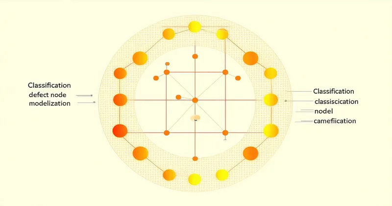
An overview of the convolutional and spatial feature extraction approach behind Wafertune's classification engine — and why training on specialty-node data changes the results.
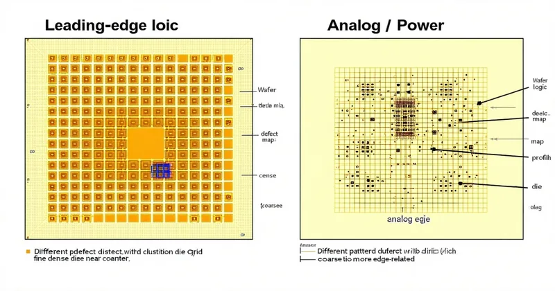
Analog and power nodes have different dominant defect mechanisms than leading-edge logic. This affects what patterns your model needs to recognize — and where generic training data fails.
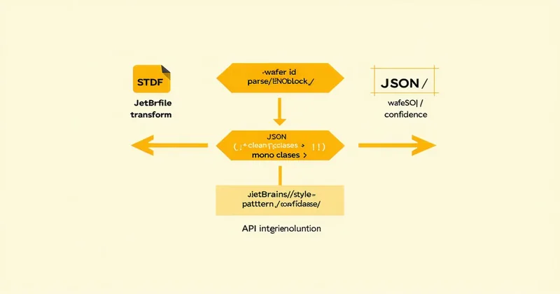
A practical guide to parsing STDF wafer-sort data and structuring it for the Wafertune classification API — common pitfalls, field mapping, and handling multi-bin maps.
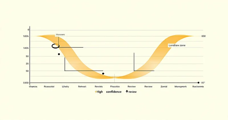
Confidence score thresholds, ambiguous patterns, and when to flag for human review — a guide to reducing false-positive alerts without missing real yield killers.

Intel, TSMC, ON Semi, and Microchip — Arizona has a growing concentration of analog, power, and specialty semiconductor manufacturing. What this means for yield analytics tooling.