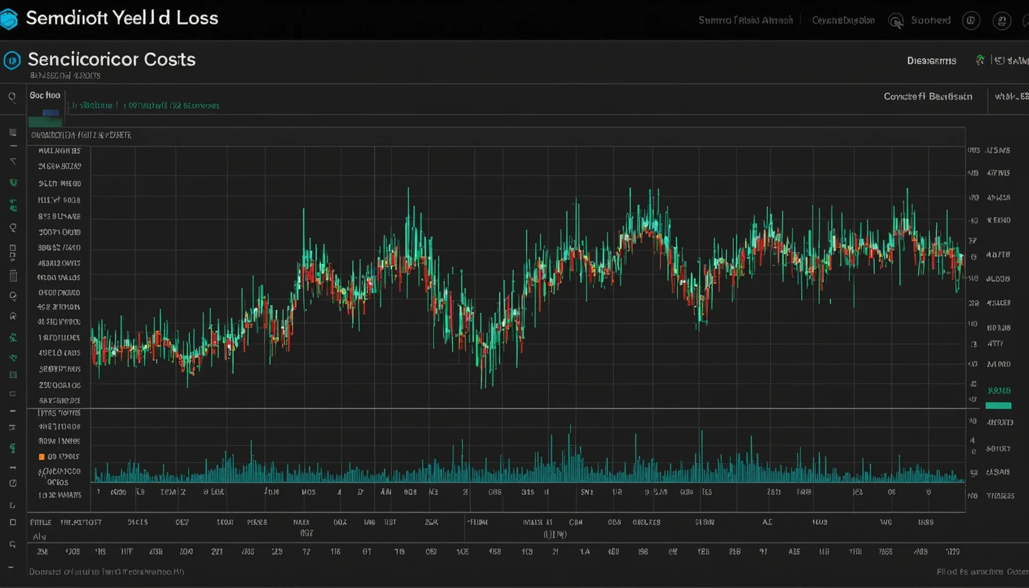
Demand for 200mm capacity hasn't cooled the way some expected. If anything, it's gotten tighter. Across analog mixed-signal, power discrete, and MEMS device categories, utilization at specialty fabs has stayed stubbornly high through 2025, and the yield pressure that comes with that utilization is a real operational problem, not a planning footnote.
What's Keeping 200mm Lines Busy
Three demand vectors stand out in our tracking. First: EV powertrain content. Each battery electric vehicle contains roughly 2 to 3 times the power semiconductor content of a comparable internal-combustion platform. That translates directly to sustained demand for 100V to 600V power MOSFETs, IGBTs, and gate drivers, most of which are still produced on 200mm lines using established CMOS and BCDMOS process flows. Second: industrial automation. We've seen pull-through demand from motor drives, robotics controllers, and programmable logic controllers that has kept analog mixed-signal capacity pinned above 90% utilization at several major IDMs. Third: the MEMS category continues to grow steadily, driven by automotive sensor proliferation, medical devices, and consumer wearables.
None of these demand sources are going away before 2027. That matters for yield management because high utilization changes the risk calculus. When a fab is running at 95% capacity, holding wafers for extended diagnostic cycles isn't a yield engineering preference, it's a scheduling conflict. Lots move. Excursions get shorter investigation windows. And that's where things start to compound.
Why 200mm Fabs Can't Reuse Advanced-Node Yield Playbooks
There's a persistent assumption in some quarters that yield management tools developed for 5nm and 3nm fabs should translate cleanly to 200mm specialty nodes. They don't. Not really.
The process physics are different. At 90nm to 180nm, feature variation tolerances are wider relative to leading-edge, but the device types running on a single line are far more heterogeneous. A single 200mm fab might run high-voltage bipolar processes alongside standard CMOS alongside thick-oxide devices for analog I/O. Each of those flows has different defect sensitivity windows, different thermal budgets, and different metrology targets. The defect signature for a MOSFET threshold shift looks nothing like a gate oxide pinhole in a 200V DMOS transistor.
Practically, this means pattern libraries built on leading-edge DRAM or logic data don't transfer. Wafer map signatures that indicate a reticle defect in a 5nm logic process often look identical to a chuck contamination event at 150nm analog. Our data shows that mis-classification rates on reused pattern libraries from advanced-node environments can run as high as 40% in the first 90 days of deployment at a specialty node. Honestly, that's worse than manual classification in many cases.
Specific Yield Challenges at 200mm Nodes
Three challenge categories come up repeatedly when we talk to yield engineers at 200mm analog and power fabs.
Mixed device types on one line. A fab running both 40V BCD and 600V IGBT processes on the same physical line deals with fundamentally different yield loss mechanisms simultaneously. The process steps interleave, the maintenance schedules overlap, and a contamination event that affects one flow may present very differently in the other. Without process-aware split in the data layer, you're looking at aggregate yield curves that obscure the actual excursion source.
Wider variation tolerance windows creating detection latency. Because analog and power devices tolerate wider process windows by design, parametric excursions can drift for longer before they breach bin limits. We've seen fabs run 6 to 8 lots into an excursion before the parametric fallout shows up in electrical test data. By that point, you're looking at 15 to 20 wafers potentially affected. The same excursion at an advanced logic node would have breached CD-SEM control limits in the first or second lot.
High-mix scheduling friction. A 200mm specialty line running 40 to 60 active product flows faces scheduling complexity that single-flow DRAM fabs simply don't. Preventive maintenance windows are contested across process owners. Particle excursions from one high-volume product flow contaminate toolsets shared with a low-volume specialty product. Yield engineers spend disproportionate time on lot genealogy reconstruction rather than statistical analysis. Time consuming. Exhausting. And still the default at most fabs.
Where Diagnostic Gaps Concentrate
In our experience, the hardest part isn't identifying that a yield problem exists. Electrical test data eventually surfaces it. The hard part is closing the loop between the excursion signal and the root cause fast enough to protect the next lot.
Two structural gaps show up consistently.
Multi-tool data silos. Most 200mm specialty fabs have measurement and process data living in at least 4 to 6 separate systems: an SPC tool (often legacy), a defect inspection system, a parametric test database, a lot tracking system, and in some cases a separate EDA environment for failure analysis. These systems rarely talk to each other in real time. A contamination signal that shows up in the defect inspection tool at inline inspection may not reach the yield engineer's desktop for 8 to 12 hours, by which point two more lots have passed through the suspect toolset.
No dedicated yield team structure. At larger fabs running advanced logic nodes below 10nm, dedicated yield integration teams sit between process engineering and device engineering. At most 200mm specialty fabs, yield engineering is either a part-time hat worn by process engineers or a small team with coverage responsibilities spanning dozens of product flows. There's no bandwidth for proactive pattern analysis. Reactive triage is the operational norm. That's not a criticism of the engineers involved, it's a structural resource mismatch.
Fact: in a study of yield loss contributors across specialty analog fabs, more than 60% of excursions that exceeded a 3% yield impact were traceable to contamination events that had already been flagged in upstream inspection data before electrical fallout appeared. The data was there. The loop was just too slow to close.
What the 200mm Utilization Trend Looks Like Through 2026
Equipment suppliers and market analysts tracking 200mm fab utilization have been converging on a similar view: utilization stays above 85% through at least mid-2026 for analog, power, and MEMS capacity. Some categories, particularly silicon carbide substrates processed on 150mm to 200mm lines for automotive power applications, are effectively sold out through 2025 and into 2026 on existing capacity.
New 200mm greenfield builds are underway, but cycle times for a new fab from construction start to first production wafer remain in the 3 to 4 year range. That means the structural tightness in 200mm capacity isn't resolving in the near term.
For yield management, this has a direct implication. Fabs that were able to carry yield efficiency losses through idle capacity buffering, essentially absorbing excursion recovery time through schedule slack, no longer have that cushion. Every point of yield efficiency is now capacity efficiency. At current wafer pricing for power and analog devices, a 1% yield improvement on a high-volume product flow at a 200mm fab translates to meaningful recoverable revenue. In our modeling, that's often in the range of $500K to $2M annually depending on product mix and wafer volume.
Where This Points
The 200mm specialty fab segment has operated with significant data integration debt for years. That was tolerable when margins were thicker, capacity was more available, and product mix was simpler. None of those conditions hold now.
We've found that the highest-impact interventions at 200mm fabs aren't the most technically sophisticated ones. They're the structural changes: unifying the data layer across inspection, SPC, and test systems so excursion signals close in minutes rather than hours, and building pattern libraries calibrated to the specific device types and process flows running at each fab rather than borrowing from leading-edge logic environments.
The diagnostic gaps at 200mm analog and power fabs are real and well-documented. The good news is that they're also addressable without the multi-year modernization cycles that full fab overhauls require. The infrastructure is already there. The data is already being generated. The question is how fast the signal reaches the engineers who can act on it.