Defect Pattern Library
180+ defect signatures trained on specialty-node wafer data. Each pattern class is documented with its visual signature, process origin, and classification confidence characteristics.
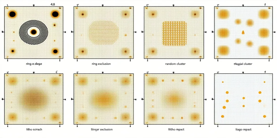
Pattern class grid
Ring of flagged dies at wafer periphery. Edge bevel contamination or edge-focused etch profile.
Diagonal line of failed dies. Wafer handling artifact or CMP pad contact.
Localized cluster without spatial regularity. Particle fallout during deposition or etch.
Periodic pattern aligned to reticle field boundaries. Reticle contamination or defocus.
Concentric rings centered on wafer. CMP pressure non-uniformity or chuck thermal gradient.
Triangular sector of failed dies. Spin-coat non-uniformity or edge bead removal issue.
Horizontal stripe of failures across wafer center. Stage vibration or deposition showerhead non-uniformity.
Concentrated failures at wafer center. Chuck contact contamination or center-heavy CMP dishing.
Vertical line aligned to wafer flat. Cassette slot contact or brush scrub artifact.
Square or rectangular block of failures aligned to reticle. Reticle particle or mask defect.
Multiple independent clusters at different wafer locations. Multiple particle sources or episodic contamination.
Wave-like alternating pass/fail bands radiating from center. CMP pad conditioning artifact.
About the classification taxonomy
Wafertune's pattern taxonomy is organized hierarchically: Spatial Category → Process Origin → Specific Pattern Class. The taxonomy was developed through analysis of wafer map datasets from specialty nodes including 200mm BiCMOS, BCD power, MEMS surface micromachining, and RF GaAs processes.
Confidence score calibration
Each classification returns a confidence score between 0.0 and 1.0. Scores above 0.85 are considered high-confidence. Scores between 0.60 and 0.85 are flagged for review — the API returns these with a review_recommended: true field. Scores below 0.60 indicate an ambiguous or compound pattern that may not match any single taxonomy entry cleanly.
Compound defect signatures in specialty nodes
BiCMOS and mixed-signal processes can produce compound defect signatures where multiple root causes overlap spatially. Wafertune's multi-label output returns the top-3 matching classes when compound signatures are detected, along with a compound_likelihood score. This is most common in LDMOS gate structures and MEMS release etch steps.
Custom pattern classes
Production tier customers with process-specific defect signatures not covered in the standard taxonomy can request custom class training. Custom classes are added to your tenant model without affecting other customers' models.
Run your wafer maps against this taxonomy.
Pilot tier: 500 free classifications per month.
Request Pilot Access