Built for specialty fabs, not just leading-edge logic.
Analog, power, RF, MEMS, and automotive-grade processes have different defect physics. Wafertune's model accounts for them.
Why specialty is different from leading-edge logic
Training data from 7nm logic fabs does not transfer to 200mm analog. The defect mechanisms, inspection cadence, and failure modes are different industries.
EUV / sub-7nm logic
- Lithography-dominated defects — stochastic EUV failures
- 300mm wafers, 12-inch standard
- Inline inspection at every layer
- Dense die grids — thousands of dies per wafer
- Large existing analytics ecosystem (KLA, PDF Solutions)
- Massive training data — billions of labeled die maps
200mm BiCMOS, BCD, MEMS
- Edge, handling, CMP, etch-profile defects dominate
- 200mm and 300mm trailing-edge mixed
- Sparser inspection — end-of-line wafer sort primary
- Coarser die grids — fewer dies, bigger die size
- Underserved by analytics tools — smaller market, less investment
- Compound signatures from multi-layer compound device structures
Six node families with trained pattern coverage
Edge exclusion, ring patterns, CMP planarization signatures. BCD and analog mixed-signal process flows.
Gate oxide scratches, thick oxide non-uniformity, drift region implant edge defects. LDMOS and DMOS structures.
Handling damage from extended inspection flows. Particle contamination from high-temperature burn-in. AEC-Q100/Q101 qualification screening patterns.
Release etch artifacts, stiction failure zones, deep etch non-uniformity. Surface and bulk micromachining. SOI MEMS patterns.
III-V material surface defects, BiCMOS buried layer edge artifacts, RF implant straggle patterns. Compound semiconductor signatures.
Capacitor dielectric non-uniformity, metal stack CMP, resistor layout edge effects. SiGe BiCMOS ADC process signatures.
Building where the specialty fabs are.
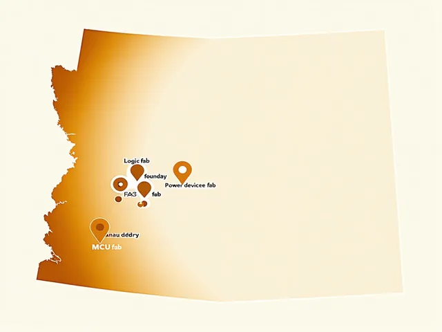
Arizona has become one of the densest concentrations of specialty semiconductor manufacturing in North America. Intel's Ocotillo campus in Chandler runs analog and mixed-signal alongside logic. ON Semiconductor's Scottsdale and Glendale fabs produce power and automotive-grade devices. Microchip Technology in Chandler and Tempe runs analog, MCU, and mixed-signal processes. TSMC's Arizona manufacturing site adds high-volume trailing-edge capacity to the corridor.
Wafertune is headquartered in Phoenix because that's where the fabs are. Founder access, customer proximity, and local process expertise shaped the model's training emphasis.
Note: Intel, ON Semiconductor, Microchip Technology, and TSMC are referenced as companies in the Phoenix regional semiconductor ecosystem. They are not Wafertune customers.
Map your fab's defect profile.
Tell us your node type and expected volume. We'll set up your Pilot API key.
Request Pilot Access